1.1 Closing the Loop
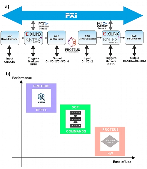
The AWT concept implemented by the Proteus platform is not just a convenient combination of an AWG and a digitizer in a single device, it is a full-fledged closed-loop processing and control solution (Figure 4.1, a). Each basic Proteus cell (4-Channel AWG @ 2.5GSa/s or 2-Channel AWG @ 9GSa/s combined with 2 Digitizer Channels @ 2.7GSa/s or 1 channel @ 5.4GSa/s and up to eight 1.25Gbps marker outputs and 2 GPIOs) incorporates a powerful FPGA from Xilinx, the UltraScale KU-060 model, tightly connected to all the analog and digital input/output blocks (Figure 1.10). The current implementation allows for the future incorporation of even more powerful and faster FPGAs. The current FPGA supports more than 700K logical cells, 2,700 DSP slices and 32 transceivers@ 16.3Gbps. The FPGA is also used by the standard Proteus functionality. The FPGA can be sued in closed-loop application in several ways (Figure 4.1, b).
The figure below depicts how Proteus units can be used for closed loop control of complex systems such as quantum computers. Loop can be closed internally through the built-in FPGA or externally through other Proteus units (or any other compatible hardware) through the high-speed (60Gbps) PCIe Gen. 3 backplane in a PXI chassis (a). The internal FPGA offers a huge unused processing capacity to implement any desired functionality in different ways (b). The standard Proteus functionality supports a “Decision Block” capable of controlling the AWG sequencer according to user-defined events coming form the analog, digital or trigger inputs. Optionally, users can obtain application-specific sets of processing blocks than can be defined and connected using SCPI commands without any need to develop IP for the FPGA. Finally, users can develop their own IP or use existing one (i.e. ARTIQ). For those users, the Proteus Shell is made available to designers so all the access to the internal HW and resources (PCIe bus, DRAM) is already designed.

Figure 1.1 Proteus Used for Closed Loop Control of Complex Systems
The first usage model does not require the implementation of application specific processing blocks, just the standard functionality. The digitizer alone can generate events through the so called “decision block”. The events generated by this bock can be used by the most powerful AWG sequencer available in the market combined with timers, external trigger events, etc. It supports conditional branching so waveforms to be outputted can be selected depending on external conditions. Dynamic sequencing (where the segment to be generated is selected by a digital parallel input port) is also possible in Proteus. The total or partial implementation of some waveform segments in the FPGA’ RAM (instead the massive DDR4 memory that can be only accessed in big blocks) greatly reduces some of the problems in high-speed AWGs with long waveform memory: trigger latency and trigger jitter.
Standard or optional application-oriented processing blocks. Multiple packages of hardware functionality will be offered. Using those, user can wire up different already defined processing blocks defined by Tabor Electronics in order to solve a specific processing chain/closed loop functionality. Instead of having to design this functionality using an eternal FPGA design tool, users can just use SCPI commands to set up the processing elements and stablish the signal flow. Some of the processing blocks (i.e. the DDC or the FIR filters) have been previously described in this paper. Some other are tightly connected to specific application areas such as quantum computing, wireless network, or Radar.
“Shell” based solutions where users design all the functionality using any available FPGA design tool while Tabor Electronics supply the IP “Shell” that provides easy access to all the Proteus HW without having to deal with all the critical timing and functional requirements related with the high-speed signals generated and acquired by the Proteus platform and the integration with the DDR4 massive RAM memory and the access to 3rd Generation 8x PCIe bus (50Gbps communication speed). This approach hides all the complexity of the Proteus platform to users while giving full freedom to designers to create their own solution. This is an ideal solution for very complex closed-loop environments and even for the prototyping of proprietary closed-loop systems.
1.2 Modularity and Scalability
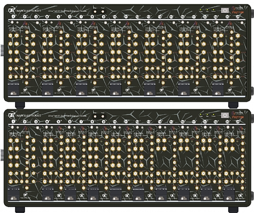
Operational quantum computing systems and other applications (i.e. massive MIMO, phase-array RADAR) may require tens of analog inputs and outputs combined with multiple digital inputs and outputs. A typical qubit may require two analog channels to control the state of the qubit and one channel to read its state at very specific, tightly controlled moments in time. Some digital signals may be also necessary as well. Just one Proteus PXI module could then control up to two qubits simultaneously. A single 21 slot PXIe mainframe can hold up to 10 AWG Proteus cards so 40 AWG channels can be supported in it (Figure 4.2). Embedded PXI controllers or external computers connected through very high-speed optical interfaces to the PCIe bus could even implement the closed-loop processing and control. The PCIe implementation in the Proteus platform, allows for sustained transfers at 50Gbps (or >6GSa/s @ 8bit resolution) from/to any external device. However, when real-time processing and low latency closed-loop control is necessary over more than a few channels, the external controller is not the answer. There are too main reasons for it. First, the PCIe bus, even in its highest performance implantations will become a bottleneck as it should be shared by multiple channels from multiple modules. Secondly, because any external computer will run out of processing power for a relatively small number of channels. There are other issues, such as the latency time (very important in close-loop control) or the deterministic behavior of the processing system. Th Proteus solution, where an FPGA is incorporated to any basic Proteus block, avoids transferring unnecessary information through the PCIe backplane while the processing power grows with the number of channels in a predictable, proportional manner. User can implement signal and data processing using a general-purpose processor implemented in the FPGA (i.e. an ARM processor) or using application-specific hardware processing or a combination of both. The traffic in the PCIe bus can be reduced to configuration, supervisory and monitoring data to/from the control computer or for information shared of transmitted between modules.
The channel density and the fact the internal processing power escalates with the number of channels make the Proteus platform ideal for applications where many input and output channels are required and may need to grow in the future. In the below figure, two Tabor PX21100 PXIe optical chassis hold a total of 17 Proteus modules of different models, both AWG and AWT. The chassis in the top includes 7 AWT modules (3 slots each) with 28 AWG channels, 14 Digitizer channels, and 56 digital (marker) outputs. The chassis in the bottom holds 9 AWG modules and 1 AWT module with up to 40 AWG channels, 2 digitizer channels, and 80 digital outputs. Multiple chassis can be synchronized to work as a single unit. The optical PCIe extender supported by this chassis allows for a 100Gbps connection to any controller so there is no need to integrate an embedded PXI controller to access the PCIe backplane at full speed.

Figure 1.2 Proteus for High Capacity and Scalable Applications